Title: "[[From-Gates-to-Circuits-II-Sequential-Circuits]]"
Author:
- AllenYGY
status: DONE
tags:
- NOTE
- CO
- Lec6
created: 2024-01-16T21:03
updated: 2024-05-31T01:16From-Gates-to-Circuits-II-Sequential-Circuits
Sequential Circuits
Sequential circuits’ output depends not only on its current inputs, but also its previous inputs (current state)
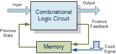
One bit memory
- It should be able to hold a single bit, 0 or 1.
- You should be able to read the bit that was saved.
- You should be able to change the bit. There are only two choices:
- Set the bit to 1
- Reset, or clear, the bit to 0.
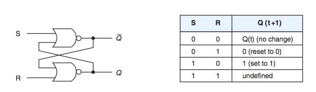
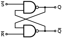
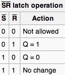
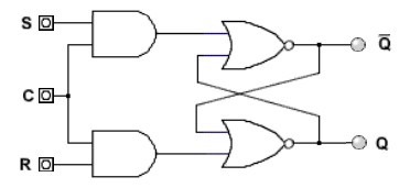
SR NOR Latch (or Flip-flop)
-
Input:
-
Output:
-
Set Function:
When
Then change -
Reset Function:
When
Then change
When
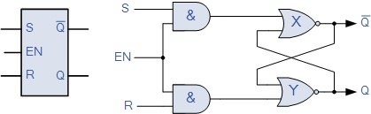
This results in a J-K flip-flop
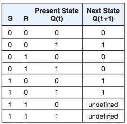
-
For inputs SR = 00, the next value of Q could be either or 1, depending on the current value of Q.
-
So the same inputs can yield different outputs, depending on whether the latch was previously set or reset.
-
This is very different from the combinational circuits that we’ve seen so far, where the same inputs always yield the same outputs.
-
4-bit latch
Gated SR Latch
- Enable 实现锁存功能
- 当Enable为0时: S,R皆为0电路锁存
SR-NAND Latch
- 与SR—NOR Latch 类似
Glitch
- There is a finite time delay between a change in the inputs of a gate and any change in the output. This time is called gate delay.(栅极延迟)
- In order to avoid glitches, we want to design storage elements that only accept input when ordered to so We use a clock to be the control input that gives orders to the circuit about when to change states
Clock
A clock is a special circuit that produces electrical pulses
Clock speed is generally measured in megahertz (Mhz), or millions of pulses per second
A clock is used by a sequential circuit to decide when to update the state of the circuit 决定何时更新电路状态
inputs to the circuit can only affect the storage element at given, discrete instances of time
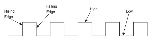
Edge-Triggered vs Level-Triggered 边沿触发与电平触发
- Edge-triggered: allowed to change their states on either the rising or falling edge of the clock signal
- Level-triggered: allowed to change state whenever the clock signal is either high or low
- Technically, a latch is level triggered, whereas a flip-flop is edge triggered
锁存器是电平触发,触发器是边缘触发
Clocked S-R Latch
- When C is 1, the circuit acts just like the NOR gate S-R latch.
- When C is 0, the Set and Reset inputs are disabled
- The latch can change only when C is true
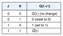
J-K flip-flop
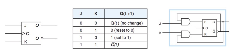
When {J=1,K=0,C=1} work like a SR latch
When {J=0,K=1,C=1} work like a SR latch
When {J=1,K=1} Q 状态反转
D flip-flop
-
It stores one bit of information
-
The output changes only when the value of D changes
-
an output value of 1 means the circuit is currently “storing” a value of 1
-
A D flip-flop is a true representation of physical computer memory
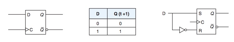
-
D 实现设置/重置 0/1
-
EN 实现 锁存 当EN为0 电路锁存
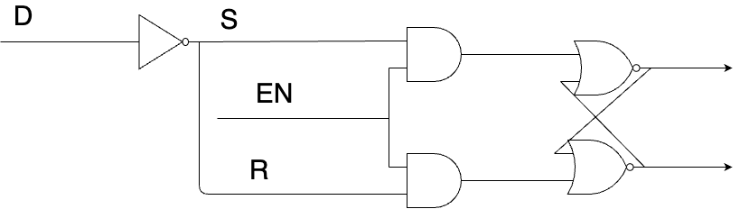
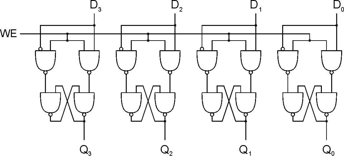
4-bit Register
- 4 input lines, 4 output lines and a WE (Write Enable) line (also called clock)
- WE实现锁定输出状态
Binary Counter
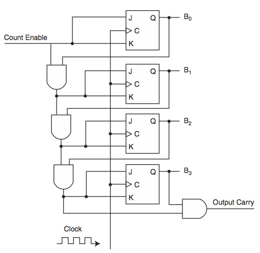
B0 (t+1) = JK (1, 1) = NOT B0(t)
B1 (t+1) = JK (B0(t), B0(t))
B2 (t+1)= JK (B0(t)B1(t), B0(t)B1(t))
B3 (t+1)= JK (B0(t)B1(t)B2(t), B0(t)B1(t)B2(t))
4 x 3 Memory
可以说是三个4-bit register组合
Decoder 选择
输出则为
以选择
- The inputs lines: In0, In1, and In2
- Address lines: S0 and S1
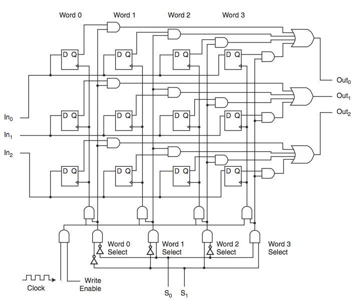
- Write a word to the memory
-
- An address is asserted on S0 and S1.
-
- WE (write enable) is set to high.
-
- The decoder using S0 and S1 enables only one AND gate, selecting a given word in memory.
-
- The line selected in Step 3 combined with the clock and WE select only one word.
-
- The write gate enabled in Step 4 drives the clock for the selected word.
-
- When the clock pulses, the word on the input lines is loaded into the D flip-flops.
Memory Addressing
- Let’s assume a very simple microprocessor with 10 address lines (1KB memory)
- Let’s assume we wish to implement all its memory space and we use 128 x 8 memory chips
- SOLUTION
- We will need 8 memory chips (8x128=1024)
- Chip selection: We will need 3 address lines to select each one of the 8 chips
- Memory location selection inside each chip: Each chip will need 7 address lines to address its internal memory cells
- Address: 000 0000000 (
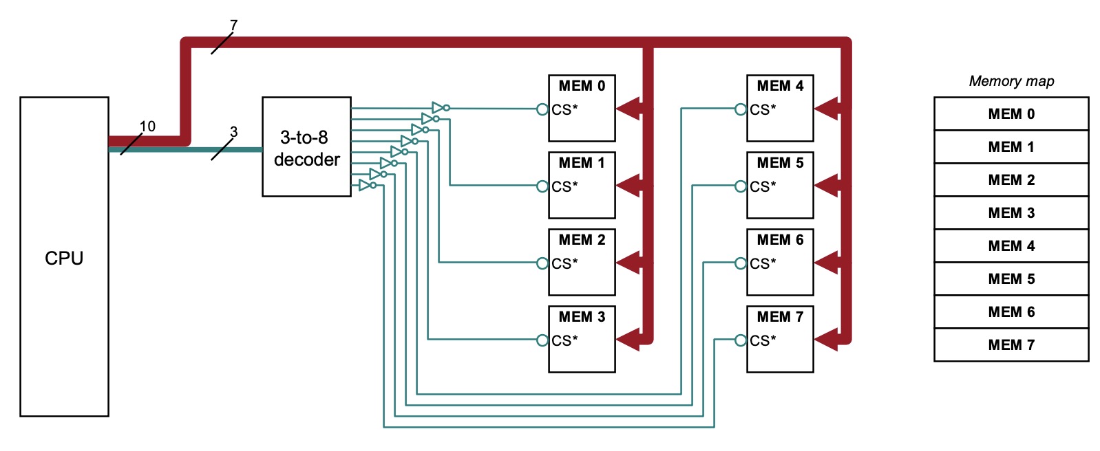 具有10根地址线的简单微处理器(可寻址1KB内存)使用128 x 8存储芯片的方法。
具体来说:
-
10根地址线的微处理器(1KB内存):
- 这个微处理器有10根地址线,这意味着它可以寻址 (2^{10}) 个不同的内存位置,可访问1KB(1千字节)的内存。
-
存储芯片:
- 为了覆盖整个内存空间,选择了128 x 8存储芯片。每个芯片的容量为128个存储位置(128个地址),每个存储位置可存储8位(1字节)。
-
所需存储芯片数量:
- 由于总内存空间为1KB,每个芯片的容量为128个存储位置,因此需要总共8个芯片((1 \text{KB} / 128 \text{每芯片的位置}))来容纳整个内存空间((8 \text{芯片} \times 128 = 1024 \text{位置}))。
-
芯片选择:
- 为了选择8个存储芯片中的每一个,使用3根地址线。使用3根地址线可以选择8个芯片中的任意一个(因为 (2^3 = 8))。
-
每个芯片内存位置的选择:
- 在每个芯片内部,需要7根地址线来寻址内部存储单元。这7根线帮助选择每个芯片中128个存储位置中的特定一个。
-
地址:000 0000000:
- 这是一个示例地址。前三位数(000)用于选择8个存储芯片中的一个。剩下的7位数(0000000)用于在选定的芯片内选择特定的存储位置,其中每个芯片有128个可用的存储位置。
Summary
- Sequential circuits can remember their previous inputs
- Sequential circuits require clocks to control their changes of states
- The basic sequential circuit unit is the flip-flop: SR, JK and D flip-flop
- Examples: registers, binary counter and memory